
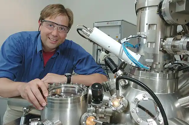
Scanning tunneling microscopes (STM) allow imaging of surfaces at the atomic level. They were developed in the 1980s and marked a breakthrough in nanotechnology, providing unprecedented views of individual atoms and molecules.
STM uses quantum tunneling to detect variations in a surface; unlike optical or electron microscopes, it does not use lenses or beams.
The Different Parts of A Standard STM
1. A Conductive Tip
An extremely sharp conductive tip, often on the order of a few angstroms (10^-10 meters) and made of tungsten or platinum-iridium, is positioned just above the sample surface. The tip sharpness determines the attainable resolution.
2. Piezoelectric Scanners
Precise piezoelectric ceramics make fine adjustments to the x, y, and z positions of the tip. Voltages applied to the piezos cause them to expand or contract to maneuver the tip.
3. Feedback Loop
Circuitry maintains a constant tunneling current by adjusting the tip-sample separation. This involves amplifying the current signal, comparing it to a set point, and generating correcting voltages for the piezo.
4. Vibration Isolation
The STM needs to be isolated from vibrations through systems like springs and magnets. This prevents extraneous tip motions that would disrupt the scanning.
5. Analysis and Display Monitor
The computer acquires data, controls the tip position and scanning, and reconstructs the surface image. The software also enables analysis and plotting.
6. Current Amplifier
Measures and amplifies the minute tunneling currents, typically picoamps to nanoamps. High-sensitivity current measurements are essential.
7. A Voltage Source
Applies a bias voltage between the tip and sample to enable the tunneling of electrons. The voltage level impacts imaging resolution and electronic structure information.
8. Sample Stage
Holds and positions the sample being imaged. May enable coarse positioning, rotation, and precision temperature control.
The Working Principle of Scanning Tunneling Microscopes
An STM has an extremely sharp conductive tip that is brought very close to the surface to be imaged, on the order of a few angstroms (10^-10 meters). When a small voltage is applied, electrons can quantum mechanically tunnel between the tip and sample surface.
The tunneling current is extremely sensitive to changes in the distance between the tip and the sample. As the tip scans across the surface, the vertical position of the tip is adjusted to keep the tunneling current constant. The adjustments in tip height are recorded and used to generate a topographic image of the surface.

How STM Differs From Standard Light and Electron Microscopes
Optical microscopes use lenses to focus visible light onto a sample. They are limited by the wavelengths of light to a resolution of about 200 nm. Electron microscopes like TEMs (transmission electron microscopes) and SEMS (scanning electron microscopes) accelerate electrons which have a much shorter wavelength, allowing imaging below 1 nm.
However, electron beams can damage sensitive biological samples. They also require high vacuum conditions. In contrast, STMs can operate at ambient temperatures and pressures, making them suitable for imaging molecules and semiconductors without damaging them.
The key difference from these other microscopes is that STM does not use lenses or beams. It relies on quantum tunneling detection, providing atomic resolution by directly interacting with the electron orbitals of surface atoms. This overcomes the limitations of optical diffraction and aberrations affecting resolution.
Applications of Scanning Tunneling Microscopy
Some major applications of STMs include:
Atomic Manipulation
Individual atoms can be precisely positioned on surfaces using an STM tip, enabling the creation of special structures atom-by-atom. This has been used to create quantum corrals out of iron atoms on copper surfaces.
Surface Analysis
STM can characterize surface defects, impurities, bonds, and electronic structures on the atomic scale. This helps inform models and improve fabrication methods for semiconductors, thin films, catalysts, and other nanomaterials.
Molecular Imaging
STM in conjunction with Raman Spectroscopy can non-destructively image delicate organic molecules, revealing detailed chemical structure and bonding configurations. STM has enabled molecular resolution imaging of DNA, proteins, and a wide range of other biologically and industrially relevant molecules.
Key Advantages of STM
- Atomic resolution of surfaces without damage from radiation
- Operation at ambient conditions for air-sensitive or biological samples
- Direct probing of surface electron states
- Ability to manipulate individual atoms
- 3D imaging capability
Limitations of STM
- Only conductive or semiconducting surfaces can be imaged
- Rough or irregular samples are challenging
- Lateral resolution depends on tip sharpness (typically 0.1-1 nm)
- Imaging artifacts can occur if the tip shape changes
- Slow scanning speed relative to optical or electron microscopes
- Limited depth penetration below surface (1-10 nm)
- Requires vibration isolation
FAQ
How does an STM tip maintain a constant distance from the surface?
The tip height is adjusted using feedback loops that keep the tunneling current constant. A change in current triggers a restoring voltage applied to the tip to raise or lower it.
What kind of resolution does STM provide?
STM can image down to the atomic scale, resolving individual atoms. Lateral resolution depends on tip sharpness but can reach 0.1 nm, while vertical resolution is better than 0.01 nm.
Can STM image insulators?
No, STM requires a conductive sample surface for the electrons to tunnel between the tip and the sample. Insulating surfaces generally cannot be imaged directly with STM.
How large of an area can an STM scan?
The scanning range depends on the particular instrument but is generally on the order of 100 nm to 100 μm. Advanced STMs can scan areas up to 1 mm.