
An electron microscope uses a beam of electrons to illuminate a specimen and create an enlarged image. The image resolution attainable for electron microscopes easily exceeds that of light microscopes due to the small de Broglie wavelength of electrons.
Electron microscopes allow the examination of samples at a very fine scale—even as small as a single column of atoms. These microscopes produce the highest possible magnification among all microscopes.
Timeline Of The Development of Electron Microscopes
The electron microscope was developed in the 1930s by pioneering engineers including Ernst Ruska and Max Knoll. Ruska and Knoll constructed the first transmission electron microscope (TEM) in 1933, accelerating electrons through thin samples to achieve much higher magnification than light microscopes.
The first commercial TEMs were produced in 1939 by Siemens, and the first scanning electron microscope (SEM) was built in 1942. Since then, ongoing technological improvements like aberration correctors, electron guns, and detection systems have dramatically enhanced electron microscope resolution and analytical capabilities.
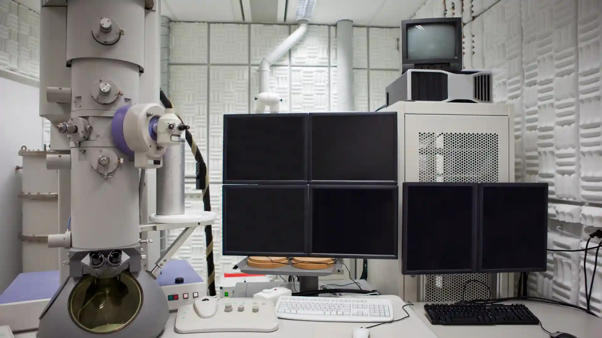
Components of an Electron Microscope
1. The Electron Gun
The first and foremost component of an electron microscope, the electron gun, contains a heated metal filament, usually tungsten, within a vacuum chamber. Thermionic emission from the filament generates a beam of electrons. The beam is accelerated by applying a positive electrical potential to an anode. Electromagnetic lenses focus the beam.
2. Electromagnetic Lenses
Electromagnetic lenses focus the electron beam using magnetic fields. They are analogous to glass lenses in a light microscope but allow for much greater magnification. Condenser lenses reduce the diameter of the beam before it strikes the sample. Objective lenses located after the sample focus the transmitted beam to form the image.
3. Sample Stage
The sample is mounted on a stage between the objective lens and the condenser lens. Precise movement allows different areas to be examined. The stage sits within a vacuum column to prevent the scattering of electrons by air molecules.
4. Detectors
Transmitted electrons passing through the sample strike a fluorescent screen, similar to the one found in a cathode ray tube (CRT) television. This builds up the image, which is captured by a camera and displayed on a monitor.
5. Vacuum System
The electron beam propagates under high vacuum conditions generated by vacuum pumps. Pressures approaching ultrahigh vacuum remove contaminant gases that would otherwise interact with the electron beam.
Types of Electron Microscope
There are two main types of electron microscopes – transmission electron microscopes (TEM) and scanning electron microscopes (SEM).
Transmission Electron Microscopes (TEM)
TEMs accelerate electrons at high voltage (80-300 kV) from an electron gun fitted with either a tungsten filament or more recently, a field emission gun. The stream of electrons is concentrated and focused using electromagnetic lenses into a thin beam just nanometers wide.
This beam is transmitted through an ultra-thin sample, interacting with sample atoms to form an image. Heavy atoms like lead or gold scatter more electrons compared to lighter atoms. Thus areas with more dense atoms appear darker in the final image.
Scanning Electron Microscopes (SEM)
In contrast to transmission mode, SEM fires the focused electron beam at the sample surface, systematically scanning point-by-point. Electrons collide with atoms in the sample, losing energy through different scattering effects.
Detectors collect the resulting backscattered electrons, secondary electrons, X-rays, and other emissions to assemble detailed 3D-like images of the surface.
For a comparative study of SEM and TEM check out our in-depth article here.
Working Principle
The working principle of electron microscopy can be divided into the following phases for a better understanding
Phase 1: Generating and Accelerating the Electron Beam
At the top of the microscope column is an electron gun, consisting of a thin metallic filament (cathode) within a metal housing (anode). Upon heating the filament, electrons are released via thermionic emission.
A strong electric potential of 0.1-30 kV is applied between the cathode and anode, accelerating electrons to high velocities and focusing them into a narrow beam. In some microscopes, Field Emission Guns (FEGs) replace heated filaments for superior coherence and brightness.
Phase 2: Electromagnetic Lenses and Apertures
The beam travels down the column through a series of magnetic coils and metal apertures that focus and confine the electrons using electromagnetic principles into a thin, tight, coherent beam just nanometers wide.
These condenser and objective “lenses” dynamically focus and deflect the electrons, scanning them across the sample surface (SEM) or transmitting through thin areas (TEM).
Phase 3: Electron Sample Interactions
When electrons strike the sample, they undergo various interactions:
- Transmission – electrons pass through thin areas of the sample largely unimpeded. This provides information about the sample structure and density.
- Backscattering – electrons elastically reflect, providing information on the composition and crystallographic structure.
- Secondary emissions – inelastic collisions excite electrons within sample atoms that are ejected as secondary electrons. This provides topological and compositional information.
- X-ray emissions – inner shell ionization creates characteristic X-rays that reveal elemental composition.
Phase 4: Imaging Construction
For TEM, areas with greater density appear darker. For SEM, the various electron emissions reveal detailed 3D surface structure. Sophisticated computer software processes signals, handling image optimization, scan control, data representation and user interfaces.
Together these components allow modern electron microscopes to achieve outstanding magnification from 10x to 2 million x along with sub-nanometer image resolution!
Cost of Electron Microscopy
High-end electron microscopes typically cost over $500,000. Significant infrastructure including stable electrical supplies, cool water, and vibration isolation are also required. Operating budgets must account for consumable parts, sample prep materials, and highly trained personnel.
For a better overview of the costs of electron microscopes check out our article.
Advantages of Electron Microscopes over Light Microscopes
One of the major advantages that Electron microscopes have over light microscopes is their much higher resolving power due to the short wavelength of high-energy electrons.
Light microscopes are limited by the wavelength of visible light to resolutions of about 200 nm. In contrast, the electron microscope resolution can be 0.05 nm or better, allowing visualization of individual atoms.
Other notable advantages include:
- Large depths of field allow more of a specimen to be in focus.
- Higher magnification from stronger electron lens focus.
- Enhanced contrast from multiple imaging modes.
- Elemental analysis capabilities from emitted X-rays.
Key Limitations Associated with Electron Microscopy:
Limited field of view
The field of view even at lower magnifications is extremely small, making it challenging to correlate small area images with overall sample structure without multiple images.
At the highest resolutions, only tiny areas <500 nm across can be imaged which poses difficulties in obtaining morphological context. Advanced microscopes with sophisticated image mapping, scanning, and stitching capabilities help mitigate such issues.
Constrained environments
All forms of electron microscopy demand high vacuum conditions within the column, as well as often requiring delicate instrumentation and infrastructure. This hinders the examination of living organisms, dynamic reactions, and systems requiring realistic environments.
Certain specialized electron microscopes allow marginal improvements, but remain challenging and still utilize high vacuum operation overall.
Complex, technique-sensitive sample preparation
Especially for transmission electron microscopy, the sample preparation steps involving chemical fixation, dehydration, staining, embedding, and ultra-thin sectioning can easily damage delicate nanostructures or leach important chemicals from the specimens.
Each step must be carefully optimized for the given sample to minimize preparation artifacts in the resulting EM images. The technique itself requires highly skilled expertise.
Challenging quantitative image analysis
Extracting quantitative information beyond basic imaging remains difficult, especially in determining detailed sample compositions, electronic properties, and bonding configurations.
Modern advances in analytical EM techniques including EDX, EELS, and HAADF imaging alleviate such issues to some degree, but quantitative analysis is still complex.
Limitations for beam-sensitive materials
A host of technologically relevant materials like organic photovoltaics, tissue scaffolds, and high-strength polymers undergo beam damage or alteration during analysis. At higher magnifications, ionizing radiation essentially fries delicate nano-features.
Applications Of Electron Microscopy
Electron microscopy empowers researchers across disciplines through its exceptional magnification range and resolving power for nanostructures:
- Materials Science: Electron microscope analysis of metals, semiconductors, and composites reveals the origins of material properties and failure modes. Fracture behavior, grain sizes, thin film deposition, and contamination sources represent just some of the areas advanced by electron microscopy techniques.
- Structural Biology: Structural biologists rely extensively on transmission electron microscopy (TEM), in conjunction with X-ray crystallography, to determine macromolecular assemblies down to near-atomic resolutions. Landmark examples include deducing ribosome, microtubule, and membrane protein structures central to cellular function.
- Microbiology: Electron microscopy allows direct imaging of cell surfaces, internal structures, and viruses in remarkable detail. Tracking infectious disease mechanisms, developments of medical cures, and gaining a basic understanding of life processes all benefit from electron microscopy imaging.
- Semiconductor Industry: Scanning and transmission electron microscopy are Routinely used to inspect silicon wafers, nano-scale device components, interconnects, and cross-sections during microchip fabrication and failure analysis. Composition, contamination, crystalline defects, and electrical properties can all be examined.
- Nanoparticle Research: The size, shape, and surface morphology of nanoparticles play critical roles in dictating their functionality. Electron microscopy provides direct geometric and compositional characterization of nanoscale catalysts, drug carriers, optical tags, and electronic materials under development.
- Food Science & Agriculture: High magnifications allow examination of microbial contaminants, macromolecular changes during food processing, and intrinsic structures within edible plant tissues – aiding quality control and agricultural R&D efforts.
- Forensics: Miniscule forensic evidence including gunshot residue, traces of dust, pollen, or hair samples, and engraved tool markings on surfaces can provide clues within criminal investigations. Scanning electron microscopy visualizes such specimens.
- Tribology & Mechanical Testing: Fractography leverages electron microscopy to determine failure modes and crack propagation details within structural materials, assisting optimization of alloy compositions and manufacturing processes. Mechanical wear over time is also well characterized.
- Clinical Pathology: Visualizing sub-cellular physiological effects of diseases and the rapid detection of pathogens are vital medical applications of EM. Fine structural details aid significantly in diagnosing patient conditions compared to optical microscopy alone.
FAQ
What is the typical magnification range for electron microscopes compared to light microscopes?
Electron microscopes commonly achieve magnifications of 50,000x to 2 million x, while light microscopes are generally limited to 1000x to 2000x magnification.
How are samples prepared for viewing with an electron microscope?
Samples require special preparation like fixation, dehydration, staining, and sectioning into ultra-thin slices less than 100 nm thick using an ultramicrotome.
Why must electron microscopes operate under vacuum conditions?
Air molecules scatter electrons, reducing image clarity. The high vacuum minimizes contaminants that can interact with the electron beam.