
Atomic force microscopy (AFM) has become an indispensable tool for nanoscience research and nanotechnology developments. Invented in the 1980s, it overcame the limitations of traditional light and electron microscopes by using a mechanical probe to scan surfaces. AFM opened up new possibilities for imaging, measuring, and manipulating matter at the nanoscale.
Atomic force microscopy (AFM) is a type of scanning probe microscopy that allows for nanoscale imaging and measurement of surfaces. AFM utilizes a sharp probe to scan over a sample surface, interacting with the atoms on the surface and mapping out the topography with extremely high resolution.
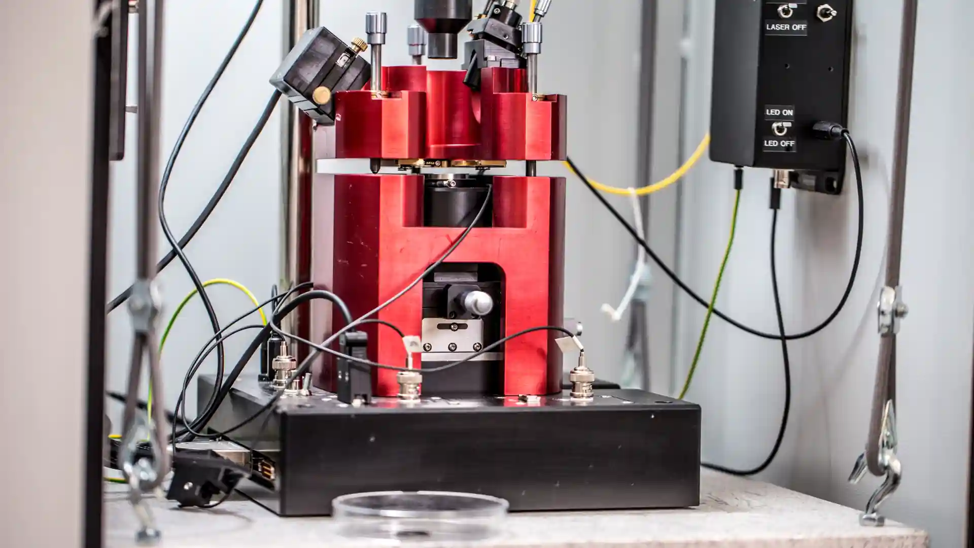
The Different Working Components of An AFM
Microcantilever
A microcantilever with a sharp tip at its end is used to scan the specimen surface. The cantilever is commonly made of silicon or silicon nitride with a tip radius of 5-10 nm.
Tip
The sharp tip at the end of the cantilever interacts with the sample surface. Tip radius, shape, and coating determine resolution and capabilities.
Piezo Scanner
A piezoelectric scanner moves the cantilever and tip in 3 dimensions over the sample surface. Allows for precise scanning motions.
A Laser Source
A laser beam is reflected off the back of the cantilever onto a photodetector to measure cantilever deflections.
Photodetector(s)
Detects movements of the reflected laser beam to measure the bending and twisting of the cantilever as it scans.
Controller/Processor
Computer and electronics control the scanner motion, laser, and photodetector. Also processes signals to generate surface images.
Mobile Stage
A movable sample stage allows for course positioning of the sample under the cantilever tip. Stable low-vibration stages are essential.
Isolation Pillars
The AFM body sits on isolation supports and platforms to damp vibrations from the environment. Critical for high-resolution imaging.
The Working Principle Of Atomic Force Microscopy
As the tip of the AFM scans across the sample surface, forces between the tip and sample cause the cantilever to deflect. This deflection is measured by reflecting a laser beam off the cantilever onto a photodetector. (as shown in figure 1)
The measured cantilever deflections allow a computer to generate a topological map of surface features. Depending on the forces between the tip and sample, AFM can be operated in contact mode, non-contact mode, or intermittent contact mode. Advanced AFMs can also measure other forces such as magnetism, friction, and electrostatics.

Comparison to Other Microscopic Techniques
Unlike optical microscopes that use lenses and light waves, AFM utilizes a mechanical probe to image and measure samples. This removes the diffraction limit of light, allowing much higher resolution on the order of fractions of a nanometer. AFMs can image insulating or conductive surfaces, unlike electron microscopes that require conductive samples.
AFM also differs from scanning tunneling microscopy (STM) which uses quantum tunneling current to image surfaces. While STM is limited to conducting or semiconducting surfaces, AFM can measure insulators. AFM can also measure a wider range of forces and properties beyond just topology.
Applications of AFM
The high resolution and flexibility of AFM has made it a versatile tool for nanoscience. Major applications include:
Topographic Imaging
AFM in conjunction with TERS generates 3D topographic maps of surfaces at near-atomic resolution. This allows imaging of everything from polymer structures to DNA molecules.
Mechanical Properties
AFM can measure nanomechanical properties including adhesion, stiffness, elasticity, and hardness of samples by analyzing force-distance curves.
Manipulation
AFM tips can manipulate individual atoms and molecules, enabling nanofabrication and molecular engineering.
Electrostatic Forces
Electrostatic force microscopy measures local electrostatic properties and charges of surfaces. Applications include imaging charge transport in electronics or nanomaterials.
Chemical Force Mapping
By functionalizing AFM tips with particular chemical groups, chemical force mapping can measure specific molecular interactions and map the chemical composition of surfaces.
Advantages
Key advantages of AFM include:
- Extremely high resolution, enabling atomic-scale imaging
- Can measure insulating and biological samples
- Provides 3D surface profiling
- Measures a variety of forces and properties beyond just topography
- Can manipulate and modify surfaces
- Works under different environmental conditions like gases, liquids, or vacuums
Drawbacks
Limitations of AFM include:
- Small scan areas, typically a few hundred microns maximum
- Slower scanning compared to electron microscopy
- Image artifacts can result from tip-sample interactions
- Specialized tips are required for some measurements
- Challenging for rough or highly sloped surfaces
Proper experimental design and calibration are needed to produce accurate AFM results. Still, when atomic-scale resolution or specialized force measurements are required, AFM is an indispensable nanotechnology tool.
Frequently Asked Questions
How does AFM compare to scanning electron microscopy (SEM)?
While SEM utilizes focused beams of electrons to image surfaces, AFM uses a mechanical probe to physically scan the sample. This allows AFM to achieve higher resolution, measure 3D topography, and image insulating/biological samples. However, SEM has higher throughput and can scan larger areas more quickly.
What types of samples can be imaged with AFM?
AFM can image almost any type of sample surface, including insulators, semiconductors, conductors, polymers, ceramics, composites, glass, and biological samples. The only requirement is that the sample must be rigidly immobilized.
What is the resolution of AFM?
The highest demonstrated resolution is up to 0.1 nm lateral and 0.01 nm depth resolution, suitable for atomic-scale imaging. However, actual imaging resolution depends on tip radius, sample, and operating mode. Typical resolution under ambient conditions is 1-5 nm.
Does AFM require a vacuum-like electron microscopy?
No, one advantage of AFM is the ability to operate under various environments like ambient air, liquids, or gases. However, the highest resolutions may require vacuum conditions to minimize vibrations.
Can AFM modify or manipulate surfaces?
Yes, AFM tips can be used to manipulate individual atoms and molecules, enabling nanofabrication techniques. For example, AFM can “push” molecules around on a surface to create simple nanostructures.